

Semiconductor Wafers
Semiconductor wafers are foundational components in the electronics industry, serving as the substrate for the fabrication of integrated circuits (ICs) and other semiconductor devices. These wafers are typically thin, disc-shaped slices made from a single crystal or polycrystalline material, with silicon being the most widely used due to its excellent semiconductor properties. Silicon wafers play a pivotal role in the production of microelectronics, enabling the creation of the intricate circuitry that powers a vast array of electronic devices.
The manufacturing process of semiconductor wafers involves several critical steps. First, a single crystal ingot of high-purity sapphire, germanium, silicon or silicon carbide is sliced into thin wafers using a precision saw. These wafers undergo a series of chemical and mechanical processes to achieve a smooth, flat surface and consistent thickness. The resulting wafers serve as the canvas for the creation of semiconductor devices through photolithography, etching, and deposition processes.
Semiconductor wafers come in various sizes, with diameters ranging from a few inches to over a foot, and their dimensions play a crucial role in determining the number of devices that can be produced in a single manufacturing run. The wafer's surface is typically polished to an ultra-smooth finish to ensure uniformity in subsequent processes.
These wafers are the platform upon which intricate patterns of transistors, resistors, and interconnects are created during the semiconductor fabrication process. The properties of the semiconductor material, as well as the precision in wafer manufacturing, directly impact the performance and reliability of the electronic components produced. Semiconductor wafers are essential in driving technological advancements across various industries, from consumer electronics to healthcare, automotive, and beyond, making them a critical element in the modern digital age.
Indium Phosphide (InP) Wafers
Indium Phosphide (InP) Wafers
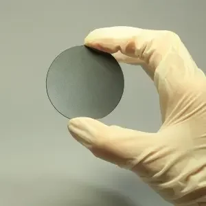
Firebird Optics’ Indium Phosphide (InP) wafers are high-quality semiconductor substrates designed for advanced optoelectronic and high-speed electronic applications. InP offers a direct bandgap of ~1.34 eV and excellent electron mobility, making it ideal for fabricating lasers, photodetectors, modulators, and high-frequency integrated circuits. With superior lattice matching to InGaAs and related alloys, InP wafers are essential in fiber-optic communications, 5G/6G networks, high-speed transistors, and infrared sensing.
Firebird Optics mostly provides these in custom configurations. Please contact us for a quote at info@firebirdoptics.com.
Specs for Indium Phosphide (InP) Semiconductor Wafers:
Indium Phosphide Wafers: Enabling High-Speed Photonics and Electronics
Indium Phosphide (InP) wafers are advanced III–V semiconductor substrates that play a critical role in modern optoelectronics and high-speed communications. With a direct bandgap of ~1.34 eV and exceptional electron mobility, InP offers performance advantages over silicon and even gallium arsenide in certain applications. These wafers are the foundation for devices used in fiber-optic networks, high-frequency electronics, infrared sensing, and emerging 5G/6G technologies.
Material Properties of InP
Indium Phosphide’s unique physical and electronic characteristics make it indispensable in photonics and high-frequency systems:
Bandgap: ~1.34 eV at 300 K (direct), enabling efficient light emission and absorption in the near-infrared spectrum (~0.9–1.7 μm).
Crystal Structure: Zinc blende cubic, offering high-quality epitaxial growth.
Lattice Constant: ~5.868 Å, perfectly matched with InGaAs and InAlAs ternary alloys.
Electron Mobility: ~5,400 cm²/V·s, higher than GaAs, enabling ultra-fast device operation.
Thermal Properties: Moderate conductivity; requires careful heat dissipation in high-power designs.
Optical Transparency: Strong transmission in the near-IR, aligning with telecommunication wavelengths.
Together, these properties allow InP to serve as the substrate of choice for fiber-optic components and high-speed integrated circuits.
Manufacturing Process
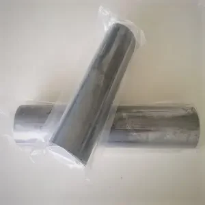
1. Crystal Growth
High-purity InP single crystals are typically produced using:
LEC (Liquid Encapsulated Czochralski): Most common growth method, preventing phosphorus loss during melting and pulling.
VGF (Vertical Gradient Freeze): Produces lower dislocation densities, improving wafer quality for demanding epitaxy.
2. Wafer Fabrication
Slicing: InP boules are sliced into wafers with standard diameters of 2″, 3″, and 4″, with 6″ emerging for advanced fabs.
Edge Profiling & Lapping: Reduces wafer stress and ensures dimensional accuracy.
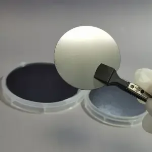
Polishing: Double-side polishing (DSP) and chemical-mechanical polishing (CMP) deliver epi-ready surfaces.
Surface Prep: Wafers may be supplied as as-cut, etched, polished, or epi-ready for MOCVD/MBE growth.
3. Doping & Conductivity
n-type: Common dopants include sulfur and selenium.
p-type: Zinc and cadmium are frequently used.
Semi-insulating: Available for specialized high-frequency and isolation requirements.
Applications of InP Wafers
Fiber-Optic Communications
InP is a key material for lasers, modulators, and detectors operating in the 1.3 μm and 1.55 μm telecom bands. It enables long-distance, low-loss optical fiber systems critical to data centers, internet backbones, and 5G networks.
High-Frequency Electronics
Thanks to its high electron mobility, InP supports heterojunction bipolar transistors (HBTs) and high-electron-mobility transistors (HEMTs) that outperform GaAs in speed and efficiency. These devices are widely used in satellite communications, radar, and mmWave systems.
Infrared Imaging & Sensing
InP substrates allow growth of InGaAs photodetectors, which cover the near-IR range up to ~1.7 μm. Applications include night vision, LIDAR, medical diagnostics, and environmental monitoring.
Emerging Technologies
5G/6G & Beyond: InP-based ICs are being developed for ultra-high-frequency, low-noise communications.
Quantum Photonics: InP serves as a platform for integrated quantum devices such as single-photon sources and detectors.
Energy Systems: Research is exploring InP’s potential in high-efficiency photovoltaic cells and thermoelectric devices.
Typical Specifications
Diameters: 2″, 3″, 4″ (6″ under development).
Orientations: <100>, <111>, with ±0.1–0.5° tolerances.
Conductivity: n-type, p-type, semi-insulating.
EPD (Etch Pit Density): <3,000 cm⁻² for premium quality.
Surface Finish: Double-side polished, epi-ready Ra < 0.5 nm.


